
The Inference Cost Case: Why Token Economics Drive Chip Design
Custom silicon's primary value proposition is not raw throughput — it is per-token compute cost at scale. When a company serves hundreds of millions of API calls per day, the economic relationship between compute hardware and output pricing becomes a first-order engineering constraint. NVIDIA operates with gross margins exceeding 70% on its data center GPU business, which means every GPU-hour a model provider purchases absorbs a significant embedded markup — one that either flows to customers through API pricing or compresses gross margin. At the scale Mistral is targeting, that structural cost becomes worth engineering against.
Mistral reported annualized recurring revenue exceeding $400 million as of February 2026, with a stated target of $1 billion in annual revenue by end of 2026 . At that revenue scale, inference serving margins stop being an operational footnote and become a material financial lever. A meaningful reduction in compute cost per token — achievable through custom silicon tuned to a specific model architecture — maps directly to either higher gross margin or the ability to lower API prices and capture market share from competitors still running on commodity hardware at full NVIDIA cost.
Mensch made the economic logic explicit in his CNBC comments, stating that proprietary chips allow a company to "lower the cost of deploying tokens to meaningful extents" . This is the same calculation that drove Google, Amazon, and Microsoft to invest in custom accelerators: at sufficient token volume, the non-recurring engineering cost amortizes and the per-token advantage compounds across every inference call served. The question is not whether the economics work in principle — they do — but whether Mistral's volume trajectory and capital structure make the investment rational within a feasible timeline.
There is also a strategic dimension to the cost argument that goes beyond margin arithmetic. Model providers who own their compute substrate can co-optimize hardware and software in ways that are structurally unavailable to GPU customers. They can tune memory bandwidth allocation, arithmetic precision formats, and on-chip SRAM sizing to match their models' specific attention patterns, layer configurations, and sequence length distributions. This is how Google achieved its inference efficiency advantage on TPU v4 and v5 workloads: not just through lower silicon cost, but through hardware-software co-design that NVIDIA's general-purpose architecture cannot replicate for a specific customer's workload. Mensch is signaling awareness of that structural advantage — not yet a program to capture it.
Hyperscaler Silicon Playbook: TPU, Trainium, and Maia Compared

Google's Tensor Processing Unit program is the canonical reference for what custom AI silicon requires in practice. The TPU v1 entered production in 2016 , but architecture decisions and early design work began around 2013 — a three-year ramp from design lock to production yield at a company with Google's engineering depth and existing foundry relationships. Google is now at TPU v5e and v5p, meaning the program represents over a decade of continuous investment, architectural iteration, and silicon-software co-development. That timeline is not a warning against custom silicon; it is a calibration of the organizational depth required to execute it successfully.
| Hyperscaler | Chip | First Production | Primary Use Case | Key Claim | Sold Externally? |
|---|---|---|---|---|---|
| TPU v1 → v5e/v5p | 2016 | Training & inference | 10+ year iterative program; software-hardware co-design advantage | Yes (GCP) | |
| Amazon | Trainium | 2021 | Training | EC2 Trn1 instances; reduced AWS NVIDIA dependency | Yes (AWS) |
| Amazon | Trainium2 | 2024 | Training | ~50% cost reduction vs equivalent GPU on matched workloads | Yes (AWS) |
| Microsoft | Maia 100 | 2024 | Internal inference | Announced 2023, deployed 2024; Copilot and Azure OpenAI workloads | No |
Amazon's Trainium program illustrates the minimum viable path for a well-resourced organization. AWS announced the original Trainium in 2021 and shipped Trainium2 in 2024, with a stated target of approximately 50% cost reduction against equivalent GPU compute on training workloads . The three-year gap between generations — with full AWS engineering depth, established TSMC relationships, and existing AWS networking and data center infrastructure — sets a reasonable floor for timeline expectations for any new entrant. A startup without those pre-existing organizational advantages should expect the upper end of the 3-5 year range, not the lower end.
Microsoft's Maia 100 chip was announced at Ignite 2023 and deployed for internal Azure inference in early 2024 . Unlike TPU and Trainium, Maia is not available externally — it represents pure internal cost reduction for Microsoft's inference serving across Copilot and Azure OpenAI workloads. This design choice is instructive: even Microsoft, with a multi-trillion-dollar market cap and decades of hardware engineering capability, positioned its first AI ASIC as an internal efficiency play rather than a merchant silicon product. The first generation of custom AI silicon typically serves as a cost-reduction instrument and organizational learning vehicle, not a product line.
All three programs share a structural requirement: 3-5 years from architecture decision to production yield, plus substantial non-recurring engineering investment, before useful silicon ships at volume. These timelines reflect physics and process, not organizational inefficiency. A 3nm or 5nm tapeout at TSMC costs in the range of $50M–$200M in mask sets alone, before packaging, functional validation, yield development, and software stack construction. Building the software stack — compilers, runtimes, debugging tools, model-specific kernels — often takes as long as the silicon work itself and requires a different engineering skill set. Custom silicon is not a procurement decision. It is a multi-year infrastructure program that requires board-level capital commitment and a silicon engineering organization that itself takes years to recruit and develop.
Mistral's Current Stack: GB300 GPUs, $830M Debt, and the Compute Baseline
Mistral's current compute posture is GPU-first in every measurable dimension. The company secured $830 million (€750 million) in debt financing in March 2026 from a seven-bank consortium — BNP Paribas, Crédit Agricole CIB, HSBC, MUFG, Bpifrance, La Banque Postale, and Natixis CIB — specifically to build a dedicated AI data center at Bruyères-le-Châtel, south of Paris. That facility is being equipped with 13,800 Nvidia GB300 (Grace Blackwell) GPUs , delivering 44 MW of compute capacity, with operations scheduled to begin in Q2 2026.
"Owning the chips may come, I think it should come at some point, but for now we are relying on Nvidia, which is a great partner to us, and we're testing a few things here and there." — Arthur Mensch, CEO at Mistral AI (source: CNBC, 2026-05-28)
The debt facility is structured around specific hardware procurement rather than general operating capital. That means the $830M commitment is already deployed into a multi-year Nvidia dependency: the facility's depreciation schedule, debt service, and operational model all assume NVIDIA silicon as the compute substrate through the initial years of operation. Any custom silicon program would be additive to this baseline infrastructure — not a replacement of it — and would need to demonstrate cost advantages over hardware generations that do not yet exist rather than over today's GB300s.
The expansion roadmap extends the GPU dependency further. Mistral has announced a European capacity target of 200 MW by end of 2027 , including a secondary facility in Borlänge, Sweden through a partnership with EcoDataCenter valued at approximately €1.2 billion. Additionally, Mistral — together with Abu Dhabi's MGX fund, Bpifrance, and Nvidia — unveiled plans for a 1.4 GW AI campus near Paris , with construction slated for the second half of 2026 and operations targeted for 2028. The stated long-term compute goal is 1 GW by 2029 .
Critically, Nvidia appears as a named partner in the 1.4 GW campus announcement — not only as a vendor. That partnership framing creates an organizational and reputational relationship that makes a public pivot to competing silicon more complex than a straightforward procurement decision. The current posture is large-scale GPU procurement with exploratory silicon work running in parallel; the two are not in tension today, but a committed chip program would eventually require Mistral to manage both that relationship and its own silicon development simultaneously.
What 'Testing a Few Things' Could Mean Technically
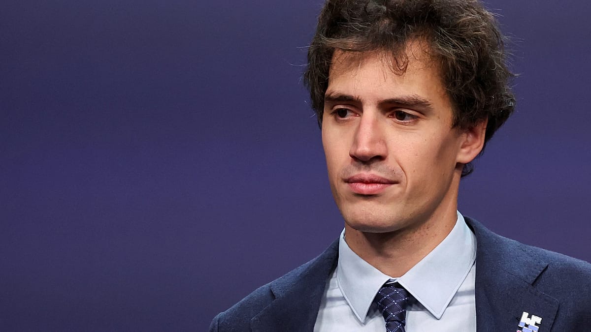
Mensch's precise phrasing — "testing a few things here and there" — is deliberately non-committal, but it maps onto a specific set of technical activities, each with different capital and timeline implications. Understanding which interpretation is most likely matters for anyone trying to read the signal accurately rather than extrapolating to a chip announcement that has not been made.
"Of course, it is interesting" — and that proprietary chips allow a company to "lower the cost of deploying tokens to meaningful extents." — Arthur Mensch, CEO at Mistral AI (source: CNBC, 2026-05-28)
Option A: Alternative accelerator benchmarking. The lowest-cost interpretation is that Mistral's infrastructure team is running inference benchmarks on non-NVIDIA hardware — AMD Instinct MI300X or MI350, Groq LPU, Cerebras WSE-3, or d-Matrix inference chips. This is standard practice for any large-scale inference operator: knowing your cost-per-token on alternative hardware is a negotiating instrument with NVIDIA and a hedge against supply constraints or pricing changes. It requires no chip design team, no NRE spend, and no multi-year commitment. It is the most natural reading of "testing a few things" in an infrastructure operations context, and it does not imply any intent to design a chip.
Option B: Co-design engagement with a fabless partner. A more ambitious interpretation is that Mistral is in early discussions with an inference-focused fabless chip firm — Tenstorrent, Etched, SambaNova, or a comparable player — around workload-specific co-design. Under this model, Mistral provides its model architecture requirements and inference workload characteristics; the partner handles RTL design, tapeout, and manufacturing. This is a lower-capital path than a full in-house ASIC program: Mistral avoids building a silicon engineering organization from scratch while still obtaining hardware tuned to its specific models. Several inference-focused silicon startups actively seek exactly this kind of anchor customer relationship to justify a focused chip design.
Option C: Early ASIC feasibility study. The highest-commitment interpretation is that Mistral has engaged a design consultancy or hired a small silicon team to perform architecture exploration and workload profiling — the preliminary analysis that precedes a tapeout decision. This would involve characterizing Mistral's model families (Mistral 7B, Mixtral MoE architectures, larger frontier models) to determine what memory bandwidth, compute density, and precision formats would maximize inference efficiency per watt per dollar. No tape-out is committed at this stage, and the team could be as small as 5-15 engineers. Mensch's statement is consistent with this activity — but so are Options A and B.
No timeline, budget, silicon architecture, or chip design partner was disclosed in the CNBC interview . That absence is informative: a committed chip program of any substance typically comes with at least directional disclosure of design goals and timeline, if only to facilitate recruiting and partnership discussions. The current statement has the structure of an options signal, not a program announcement.
The Startup Feasibility Gap: Scale, Timeline, and Capital Requirements
Custom AI silicon is financially feasible for a company of Mistral's current size under a specific and fairly narrow set of conditions: token volumes must scale significantly from today's base, a chip program must start within the next 12-18 months to deliver silicon before NVIDIA's hardware roadmap advances further, and capital markets must remain favorable enough to fund both the infrastructure buildout and a parallel silicon program simultaneously. None of those conditions is guaranteed, and the intersection of all three is a materially constrained outcome space.
| Phase | Typical Timeline | Estimated NRE Cost | Key Gate |
|---|---|---|---|
| Architecture & Workload Profiling | 6–12 months | $5M–$20M | Architecture lock; silicon team hire |
| RTL Design & Verification | 12–18 months | $30M–$100M | Pre-silicon simulation; EDA licenses |
| Tapeout (advanced-node mask set) | 3–6 months | $50M–$200M+ | TSMC or Samsung capacity booking |
| Bring-up, Yield & Packaging | 6–12 months | $20M–$80M | Silicon functional validation |
| Software Stack & Integration | 12–24 months (parallel) | $10M–$50M | Compiler, runtime, ops tooling |
| Total (full program, training-class) | 3–5 years | $100M–$500M+ | Volume production silicon |
| Mistral total equity raised (reference) | — | ~$3B | Series C at $13.8B valuation, Sep 2025 |
| US hyperscaler AI infra (2026 collective estimate) | — | ~$1T | Mensch's own public estimate |
The NRE range of $100M–$500M+ reflects a training-class chip program. An inference-only ASIC — the more defensible near-term target for Mistral, given that inference serving is where its API revenue is generated — can be designed with meaningfully lower NRE: a narrower feature set, smaller die area, and a more constrained software stack scoped to inference rather than training. Inference ASICs like Groq's LPU represent a different design philosophy than training accelerators, with correspondingly different NRE profiles. A Mistral inference co-design, if pursued, might land in the $50M–$150M NRE range depending on die size, node selection, and partnership structure — still substantial for a startup, but within the realm of a targeted fundraise rather than a program requiring hyperscaler-scale capital.
The capital comparison remains stark even under the optimistic scenario. Mistral's approximately $3 billion in total equity raised must service the $830M debt facility, fund ongoing model research and training compute, support commercial operations and sales, and — if a chip program proceeds — fund NRE and the required silicon engineering organization. US hyperscalers measured their silicon programs in tens of billions over a decade each. Mistral's total equity position is roughly the minimum threshold at which custom silicon begins to pencil economically — but only if token volumes scale 10x or more from today's base to provide the denominator that makes per-token cost improvement meaningful at an enterprise scale.
The timeline math creates an additional constraint that is easy to underweight. A program achieving architecture lock today would not produce volume silicon before 2029 under the hyperscaler baseline. By 2029, NVIDIA's roadmap includes Rubin Ultra and post-Rubin architectures. The efficiency target for custom silicon is a moving one: a Mistral ASIC must offer a durable advantage over the prevailing NVIDIA generation at the time of deployment, not over today's GB300s. That moving target means the architecture decisions made today must anticipate what NVIDIA will have in production three to five years from now — a non-trivial prediction problem.
European Silicon Sovereignty: The Policy Signal Embedded in a Technical Statement
Mensch's chip remarks did not emerge in isolation. They follow a sustained political narrative he has been constructing around European AI sovereignty, most forcefully articulated in testimony before the French National Assembly. In that testimony, Mensch warned that Europe risks becoming an AI "vassal state" within two years if it does not aggressively build independent infrastructure . A statement about custom silicon, made in this political context, carries weight that extends well beyond its technical content — and that is almost certainly intentional.
"Whoever controls the chips, whoever controls the electrons, whoever has massive access to energy — that's who wins." — Arthur Mensch, CEO at Mistral AI (source: Trending Topics)
The European Union's Chips Act targets a 20% share of global semiconductor production by 2030 . A Mistral custom chip program — particularly one built around European model architectures and aligned with European supply chain development — fits directly into that political narrative. It would position Mistral as not just a software AI company but as a potential anchor participant in European semiconductor industrial policy. That narrative alignment has real and tangible value: it makes Mistral a plausible candidate for EU and French state support, potential subsidies, and favorable regulatory treatment that a pure GPU-customer company would not attract.
The chip statement is targeting three distinct audiences simultaneously. For investors, it signals long-term thinking about inference cost structure — the kind of vertical integration that supports durable margin and a competitive moat that is structurally unavailable to pure API resellers. For Brussels policymakers, it frames Mistral as a potential anchor tenant for European semiconductor ambition, complementing Chips Act goals with a named AI workload and named European operator. For chip engineering talent, it sends a signal that Mistral may become a destination employer for silicon engineers who want to work on AI hardware without relocating to a US hyperscaler — a talent pool that exists in Europe and is currently underserved by domestic employers.
This multi-audience signaling pattern is recognizable from Meta's MTIA (Meta Training and Inference Accelerator) announcement strategy: Meta disclosed MTIA's existence and rationale well before the chip was production-ready, signaling intent to the market and recruiting talent around a stated direction before the engineering program was fully committed. Strategic signaling of this kind is common before committed R&D — it is how organizations build the organizational, financial, and political support needed for expensive long-term investments. Mensch's statement is consistent with that pattern, which makes it neither dismissible as empty talk nor readable as an imminent hardware launch.
Developer Implications: API Cost Trajectory and What to Watch

For developers building on Mistral's API, the practical question is whether any of this affects pricing, API surface, or model availability in the near or medium term. The short answer: no near-term impact, and any medium-term benefit is conditional on a committed chip program that has not been announced and a multi-year execution timeline that has not started.
Near-term (2026–2027): Mistral runs on Nvidia GB300 GPUs through at least the 200 MW European buildout planned for end of 2027 . The $830M debt facility is hardware-committed. API pricing in this window will track NVIDIA hardware economics and Mistral's volume discounts, not any custom silicon advantage. Developers should model pricing on current GPU-based infrastructure costs and expect evolution driven by Mistral's commercial scale and market competition — not chip design decisions.
Medium-term (2028 and beyond): If a co-design engagement or ASIC feasibility study matures into a committed program, inference API pricing on target workloads could compress by 20-40% compared to equivalent GPU-hosted costs — consistent with hyperscaler benchmarks for inference-optimized ASICs on matched workloads. This is contingent on a program that has not been publicly committed, execution on a multi-year timeline (historically the hardest part of any silicon program), and Mistral maintaining the token volumes needed to amortize NRE. None of those conditions is assured.
API surface stability: Custom silicon does not change model APIs. If Mistral migrates inference to custom hardware, the /chat/completions and /embeddings endpoints remain unchanged. The hardware transition is an infrastructure concern, invisible to API consumers except through latency characteristics and pricing adjustments.
Signals that indicate a real program is forming:
- Silicon architecture or hardware engineering job postings on Mistral's careers page — RTL engineers, design-for-test, physical design, and compiler engineers are hiring signals specific to a committed ASIC program
- Fabless partnership announcements — a co-design relationship would likely be disclosed as a commercial partnership, not purely as a hardware development announcement
- TSMC or Samsung advanced-node capacity bookings — chip programs require foundry slots 18-24 months ahead of tapeout; capacity booking signals commitment
- Follow-up statements with technical specificity — Mensch's current statement is a first-order signal; a second statement with design goals or timeline would indicate a program is taking concrete shape
The absence of these signals over the next 12-18 months would suggest "testing a few things" refers to Option A — alternative hardware benchmarking — rather than a silicon development program of any committed form.
Frequently Asked Questions
What exactly did Mistral CEO Arthur Mensch say about designing AI chips?
On May 28, 2026, Mensch told CNBC: "Of course, it is interesting," when asked about custom silicon, and added that proprietary chips allow a company to "lower the cost of deploying tokens to meaningful extents." He was explicit that no active program exists, stating: "Owning the chips may come, I think it should come at some point, but for now we are relying on Nvidia, which is a great partner to us, and we're testing a few things here and there." These are the first public remarks in which Mensch has directly addressed semiconductor ambitions. No timeline, budget, silicon architecture, or chip design partner was disclosed.
How long does custom AI chip development typically take from decision to production?
The hyperscaler baseline is 3-5 years from architecture lock to volume production silicon. Google's TPU program began architecture work around 2013 and reached production in 2016 — a three-year ramp with the full depth of Google's engineering organization and existing foundry relationships. Non-recurring engineering costs run $100M–$500M+ before the first production wafer, covering RTL design, verification, tapeout mask sets at an advanced node, packaging, yield development, and software stack construction. A committed program starting today would not ship volume production silicon before 2029 at the earliest under the hyperscaler timeline — and first-generation custom silicon programs routinely slip by 12-24 months beyond initial estimates.
Could Mistral co-design chips with a partner rather than build an in-house program?
Yes — co-design with an inference-focused fabless firm is a plausible lower-capital path that avoids building a full silicon engineering organization from the ground up. Companies like Tenstorrent, Etched, and SambaNova actively seek anchor customers whose workload requirements can anchor a focused chip design. Under a co-design model, Mistral would provide model architecture requirements and inference workload characteristics; the partner handles RTL design, tapeout, and production. Mensch's "testing a few things" phrasing does not exclude early vendor engagement of this kind. NRE under a co-design arrangement would be substantially lower than a full in-house ASIC program — potentially in the $50M–$150M range rather than $500M+ — making it the more capital-efficient near-term path if Mistral decides to pursue custom silicon at all.
Will Mistral's chip ambitions affect API pricing for developers in the near term?
No. The GB300 buildout at Bruyères-le-Châtel runs through at least Q2 2026, and the 200 MW European expansion is planned on the same NVIDIA hardware stack through end of 2027 . Any pricing benefit from custom silicon is a 2028-2030 story at earliest — and only if a committed chip program is announced and executes on schedule, neither of which has occurred. API surface (endpoints, model naming, authentication) is independent of underlying silicon and will not change as a result of hardware decisions. Developers building on Mistral's API today have no near-term reason to factor chip ambitions into technical or commercial planning.
How does Mistral's compute scale compare to US hyperscaler AI infrastructure investment?
The gap is substantial by any measure. Mensch himself estimated that American companies are collectively deploying approximately $1 trillion in AI infrastructure in the coming year . Mistral's stated goal of 1 GW of AI computing capacity by 2029 is significant for a European AI company — and is Mistral's own ambitious target, not a realized figure. Individual hyperscaler silicon programs (Google TPU, Amazon Trainium) represent multi-billion-dollar, decade-long investments each. Mistral's approximately $3 billion in total equity raised is the rough minimum at which custom silicon starts to pencil economically — but only under the specific conditions of significant volume growth and favorable capital markets described above.
What This Means and What Comes Next
Mensch's chip signal is best read as exactly what he described: early-stage interest, not a program announcement. The economic logic is sound — at sufficient inference scale, custom silicon generates durable cost and margin advantages that compound across every token served, and the hyperscaler precedents validate the strategy. The feasibility gap is equally real — the timeline, NRE, and organizational requirements to execute a chip program are substantial relative to Mistral's current capital position and existing infrastructure commitments. Both things are true simultaneously, and neither cancels the other.
The statement is most useful as a directional indicator of where Mistral's strategic thinking is heading: toward deeper infrastructure control, toward alignment with European semiconductor policy, and toward the hardware-software co-design that has defined the long-term competitive position of Google and Amazon in AI serving. Whether that directional intent translates into a committed program within the next 12-18 months will become readable through specific organizational signals — silicon engineering hires, fabless partner announcements, and follow-up statements with technical specificity beyond what May 28's CNBC interview provided. Until those signals appear, the appropriate interpretation is serious exploration in a pre-commitment phase.
For developers, the practical posture is unchanged: build on Mistral's API as it exists today, model inference costs against current NVIDIA-based infrastructure, and treat any cost improvement from silicon innovation as a 2028-2030 upside scenario rather than a planning assumption. The API surface will not change with hardware decisions. If a chip program materializes and succeeds, the benefit flows through as API pricing compression — straightforward for developers who do not need to track the underlying hardware to capture the benefit when it arrives.
Last updated: 2026-05-28. This article is based on Arthur Mensch's public statements to CNBC on May 28, 2026, and Mistral AI's infrastructure disclosures through March–May 2026. Chip program details, if announced, will be reflected in subsequent updates.